Ceramic Processing and Analysis Lab
Contact: Dr. Linan An
Research activities of the Ceramic Processing and Analysis Lab focus on the synthesis and characterization of ceramic materials with various length-scale, including nano-rod/belts, nano-phase reinforced composites, micro-electromechanical systems (MEMS), and bulk materials, for high temperature and harsh environment applications. Research activities are integrated with educational activities. Of particular interest is the synthesis of materials with novel structures and composites through controlling processing conditions. Collaborators on projects include other universities such as Florida State University and Tsinghua University (China), national laboratories such as Oakridge National Laboratory, Pacific Northwest National Laboratory, and several companies including Siemens-Westinghouse and Sporian Microsystem.
Equipment/Techniques available include:
- Hot isostatic pressing furnace
- High temperature furnace with environmental control
- Middle temperature furnace with environmental control
- High energy ball-milling machine
- Fisher Scientific Isotemp Muffle Furnace
- Microstereolithography set-up with inverse building capability
- Various ovens (including vacuum oven)
Nano- and Bio-Materials Lab
Contact: Dr. Jiyu Fang
The Nano- and Bio-Materials Lab focuses on the technology developments in assembly and characterization. (1) Assembly techniques include molecular self-assembly, Langmuir-Blodgett method, soft-lithography, nanosphere-lithography, scanning probe microscope patterning, and 2-D protein templates. (2) Characterization techniques are scanning probe microscopy, liquid crystal optical amplification, UV-vis, FT-IR, luorescence microscopy, and quartz crystal microbalance
Equipment/Techniques available include:
- Dimension 3100 scanning probe microscopy (Digital Instruments)
- Pico ScanTM (Molecular Imaging)
- NIMA Langmuir trough
- Nikon polarized optical microscope
- Deep UV and soft lithography
- Cantilever Sensors
- Quartz Crystal Microbalance
Crystal Growth and Epitaxy Lab
Contact: Dr. Christine Klemenz
The Crystal Growth and Epitaxy Lab (CGEL) focuses on the development of high quality bulk single crystals and epitaxial films for emerging technologies. Emphasis is especially set on new and complex materials of high potential in applications, but presenting challenging materials and growth problems. A major goal of this research activity is to achieve best device performance and reproducibility by improving existing growth and deposition processes, and by searching for new ways of synthesis. Whether large-diameter crystals, or nanocrystals and thin films, such approach is multidisciplinary in nature, and includes the study of all physico-chemical, thermodynamic, and kinetic aspects involved in the crystalliation and epitaxy phenomena. Characterization is done, among others, at AMPAC-MCF and CREOL (RBS, SIMS, TEM, SEM), crystal and wafer imaging at Brookhaven National Lab, acoustic and other crystal properties evaluations at NIST/Boulder, U.S. Army Research Laboratory.
Equipment/Techniques available include:
- Czochralski pullers for high-melting oxides (crystals up to 3 in. diameter), with RF heating and automatic growth process control
- Czochralski pullers for fluorides, with resistive heating and automatic growth process control
- Vertical Bridgman and Horizontal Gradient Freeze growth systems
- Flux, Top-Seeded Solution Growth and Liquid Phase Epitaxy furnace systems
- Single-crystal orientation, sawing, and polishing facilities
Computational Materials Lab
Contact: Dr. Patrick Schelling
Research areas include studies of thermal transport in semiconductors, including silicon,diamond and oxides, especially those of possible application to thermal barrier coatings. Current work is focused on thermal transport at the nanoscale. Using a combination of wave-packet dynamics and molecular-dynamics simulation techiques, we are beginning to learn the fundamental mechanisms of phonon transport and scattering in silicon nanowires. Other work includes a study of the interface of an oxide with water. The methodology employed is self-consistent tight-binding (SCTB). In this approach, electrons are treated quantum mechanically using a truncated basis set of atomic orbitals. Distinct from many other tight-binding models, we self-consistently include electron-electron interactions. In addition to furthering the development of electronic-structure methods, we will elucidate the redox chemistry of water at a reduced ceria surface for different choices of the ceria surface orientation.
Equipment/Techniques available include:
- Beowulf cluster with 32 slave nodes and 2 head nodes
- IGB memory per node, with each node operating at 3.06GHz
Surface Engineering/Nanomaterials Processing and Plasma Nanomanufacturing Lab
Contact: Dr. Sudipta Seal
Research activities at SEMP-NANOMAC lab include:
- Nanomaterials/thin films for sensors, coatings, optics, electrodes, membranes
- High temperature oxidation of metals, superalloys, coatings, fibers for industrial applications
- Nonlinear optical glasses
- Multiphase corrosion and inhibitor development program
- Electroless metal coatings for EMI shielding
- Chemical Mechanical Planarization of Microelectronics
Graduating students from this lab are placed in both academia and industry including Motorola, Applied Materials, Siemens Westinghouse, U.S. Navy and University of Florida. Projects at SEMP-NANOMAC are sponsored by the National Science Foundation, Agere, Florida Space Grant Consortium, Energy Strategy Associates, U.S. Filter, USNR Coal Resources, Bionucleonics, Florida High Tech Corridor and Walt Disney.
Equipment/Techniques available include:
- Fully equipped Sol-Gel Chemistry Laboratory
- Multipurpose Chemat Spincoater
- Denver Instrument 250 pH, ISE, Conductivity Meter
- Unitron Optical Photomat – 4422
- Isotemp Vac Oven – 280 A
- Thermodyne High Temp Furnace with Thermal Cycling 48000HT
- High Temperature Furnace for In-situ Oxidation Kinetics
- Lepel Induction Heating Unit
- SPECS Electron Beam Evaporator – E Flux
- Potentiostat/Falvanostat – Model 263A – EG&G Princeton with EG&G K0235 Flat Cell
- Material Processing Chamber with Cleaving, Heating, Cooling and Multiple Gas Entry System
- PHI 560 AES/ESCA system
- Access to ALS, LBNL – UC-Berkley and SLAC-Stanford Synchroton Facility
High Temperature Materials and Coatings Lab
Contact: Dr. Yong-ho Sohn
Research activities of the High Temperature Materials and Coatings Lab focus on materials science and engineering of high temperature materials and coatings. Research activities are integrated with educational activities to provide well-trained students with experimental, analytical and theoretical competency. Projects carried out include non-destructive evaluation, microstructural characterization and life prediction of thermal barrier coatings, multicomponent interdiffusion in multiphase alloys, development and life prediction of oxidation resistant coatings, and diffusion in bulk metallic glasses. These projects are sponsored by National Science Foundation (NSF CAREER DMR), South Carolina Institute for Energy Studies (SCIES) of U.S. Department of Energy (DoE), U.S. Army Research Laboratory (ARL), and several engine/materials manufacturers including Siemens-Westinghouse Power Corporation, Solar Turbine Inc., Howmet Corporation, Pratt & Whitney, General Electric Aircraft Engines, and General Electric Global Research Center. The lab is also privileged to have technical partnerships with National Institute of Standards and Technology (NIST), Argonne National Laboratory (ANL) and other universities such as the University of Connecticut and the University of Pittsburgh.
Equipment/Techniques available include:
- Renishaw RM 1000B Micro-Raman Spectrometer with Imaging CCD Detector and Ar-514nm Excitation Unit
- CM 1710 Rapid High Temperature Furnace (1700°C) with Vertical Cycling Package
- Lindberg/3M, Thermolyne and Fisher Scientific High Temperature Furnaces (1000°~1700°C) with Environmental Control
- TA Instrument Q 600 Simultaneous Thermal Gravimetric Analysis and Differential Scanning Calorimetry (S-TGA/DSC)
- Pascal Technologies Vacuum System with Hydrogen Flushing
- Nikon Optical Microscope with Nomalski Capability, MIRERO Computer-Integrated Image Capturing and Analysis System
- Automated Specimen Preparation System
Processing and Mechanical Characterization Lab
Contact: Dr. Raj Vaidyanathan
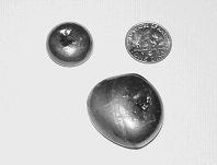
Arc melting of powders to produce button melts for nanoindentation studiesArc melting of powders to produce button melts for nanoindentation studies
The multi-scale mechanical characterization lab focuses on quantitative measurements of internal stresses with particular emphasis on: (a) in situ measurements, under externally applied loads, elevated or cryogenic temperatures; (b) multi-scale measurements, corresponding to materials both in bulk and layered/coating form. The techniques used include in situ neutron and synchrotron diffraction (performed at Los Alamos and Argonne National Laboratories) and instrumented indentation over nano-, micro- and macro-scales. In situ diffraction experiments, performed under externally applied loads and/or elevated/cryogenic temperatures, offer a unique opportunity to better understand materials by providing a valuable link between microstructural and thermomechanical phenomena. Such in situ measurements yield quantitative information on the strain, phase fraction and texture evolution. Instrumented indentation can be used to extract both local and volume-averaged properties such as modulus, yield strength, strain-hardening exponent, tensile strength and hardness. Materials studied include shape memory alloys and bulk metallic glasses.
Equipment/Techniques available include:
- MTS servo-hydraulic tester
- NanoTest 600 instrumented indenter for nano- and micro-scale testing with impact/dynamic testing, scanning, scratch and 500°C hot stage options
- Mark 14 vacuum/controlled atmosphere arc-melting and quench furnace